News

Webinar : Introducing Bruker's Next Gen Stylus Profilometer
![]() When : Tuesday 29 October 2024
When : Tuesday 29 October 2024
Time : 7pm NZDT, 5pm AEDT, 2pm AWST

We will introduce Bruker’s new 11th generation Dektak Pro Stylus Profiler, providing even more enhanced operability, reliability, and measurement accuracy to enhance and extend the qualities that make Dektak synonymous with stylus profiling.
Additionally we will explore how stylus profilers can characterise a diverse range of materials, particularly in microelectronics and semiconductor applications. Many processes in semiconductors, optical coatings, and micro-electromechanical systems (MEMS), as well as research in flexible electronics and sensors, depend on accurate thickness and etch-depth measurements. Among their various metrology capabilities, stylus profilers excel at delivering exceptional step height measurements at both the nanoscale and microscale.
Read More

Bruker Introduces Most Advanced Bencthop Stylus Profilometer
Bruker Corporation have announced the release of the Dektak ProTM stylus profilometer, the next-generation profiler in the industry-leading Dektak® product line. Incorporating over 55 years of innovation, the new benchtop system provides an expanded measurement area up to 200 mm of full-sample access for semiconductor applications, as well as a shortened time to results with improved user experience and measurement accuracy. Dektak Pro incorporates advancements that solidify the brand as the world’s most advanced stylus profiler, positioning it to address R&D, process development, and QA/QC present and future needs across a host of industrial and research markets.
Widely utilised in microelectronics, semiconductor, display, solar, medical, and materials science markets, Dektak stylus profilers are an essential precision metrology instrument found in literally hundreds of production, research, and failure analysis facilities around the world. Dektak systems are employed in both 2D profilometry and 3D surface profiling applications to measure stress, nanometer film thicknesses, and step heights with better than 4 angstrom repeatability. The new Dektak Pro introduces step height and stress measurement updates that expand its usage. A streamlined automatic step detection routine requires less user-defined parameters for a simplified analysis that reduces user-based variability. 2D stress measurement analysis is now more customisable than ever, allowing for user-defined areas and refining precision through artifact thresholds. Fast characterisation of wafer warpage and 3D stress analysis are also made possible by new automatic centering and wafer mapping features.
For further information please contact Michael Buckett or read more.
Read More
Reverse Tip Sample (RTS) Scanning Probe Microscopy
 Date: Wednesday 19 June 2024
Time: 3am NZST, 1am AEST, 11am AWST
If you are not a night owl register for the webinar and you will receive a copy after the event :)
Our guest speakers for this webinar developed Reverse Tip Sample (RTS) Scanning Probe Microscopy (SPM) to overcome the single-tip barrier of traditional SPM. By placing the sample on a tipless cantilever and the tip on the sample stage, RTS SPM essentially flips the conventional tip-sample positions.
The standout feature of this arrangement is the ability to change tips seamlessly, greatly boosting data collection efficiency in application spaces requiring frequent tip replacements. During operations in RTS configuration, the cantilever-mounted sample scans one of thousands of tips present on the probe chip. When a tip wears out, the operator repositions the cantilever onto an adjacent fresh tip, which takes mere seconds.
After a comprehensive introduction of the RTS SPM concept, this webinar will further discuss:
- Nanofabrication of probe chips and a dry etching process for fabricating high-quality Si probe chips, which features a novel tip sharpening step. The application of metal and diamond coatings on these Si probe chips will also be covered.
- Sample preparation, including dependable workflows developed for routinely preparing RTS SPM samples by focused ion beam (FIB) and FIB-less approaches. These time-efficient procedures yield RTS samples with excellent electrical contacts and mechanical stability.
- Measurements and applications of RTS SPM, such as statistical multi-tip studies, RTS Scalpel SPM, electrical tomography, and more.
Webinar Speakers:
Nemanja Peric, Ph.D., SPM Researcher, imec, Belgium
Pieter Lagrain, Engineer, imec, Belgium
Peter De Wolf, Ph.D., Senior Directory Technology & Application Development AFM, Bruker
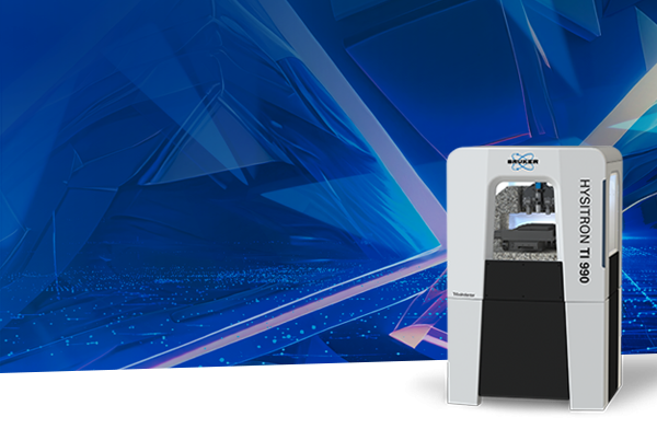
Webinar : Exploring the Future of Nanomechanical Testing with Bruker's Hysitron TI 990 TriboIndenter
![]() Day : Friday 10 May 2024
Day : Friday 10 May 2024
Time : 3am NZST, 1am AEST, 11pm AWST (Thurs 9th)
If you are not a night owl register for the webinar and you will receive a copy after the event :)
Learn about Bruker’s latest and most advanced nanomechanical and nanotribological test system, the Hysitron TI 990 TriboIndenter. Building upon a 25-year TriboIndenter legacy, the TI 990 has been completely redesigned from the ground up to deliver new levels of sample throughput, measurement control, testing flexibility, measurement reliability and performance, and ease-of-use. With an all-new system architecture and advanced testing modes, the TI 990 is set to redefine the landscape of nanomechanical and nanotribological testing.
Join us to find out:
- What is new about the TI 990 system architecture?
- What advancements are integrated into the new nanoDMA IV and XPM II?
- How is the new Performech III controller different?
- What does the redesigned TriboScan 12 software look like?
The webinar will also include a demonstration of the Hysitron TI 990 TriboIndenter.
Webinar Speakers:
David Wodnick, Bruker Nanosurfaces and Metrology
Radhika Lazminarayana, Bruker Nanosurfaces and Metrology
Webinar : Bruker's 2024 AFM Probes Webinar
Date : Wednesday 10 April 2024
Time : 3am NZST, 1am PDT AEST, 11pm AWST (Tues 9th)
If you are not a night owl register for the webinar and you will receive a copy after the event :)
Join Bruker for a short, candid webinar, where various Bruker application engineers worldwide are interviewed on what their favorite, go-to probe is and why. They will also virtually visit various demonstration labs to get tips and tricks from dedicated BioAFM, nanoIR, and automated AFM application engineers. You'll definitely discover some new probe types and maybe new ways to use legacy types!
Webinar Speakers : Ian Armstrong, Ph.D., Bruker
Read More